- Details
- Written by: Jari Ojala
- Category: Uncategorised
- Hits: 780
Vds overcurrent protection and current measurement board
The circuit board has Ids current measurement functions, as well as fast shutdown in overcurrent situations.
The overcurrent can be adjusted as desired with a trimmer. Vds voltage on/off control. Locked shutdown in overcurrent situations. Output signal indicating locking. The locking is removed by resetting with a reset signal.
One board has two separate protection/measurement lines. The board is suitable for two amplifiers containing 1-2 RF modules.

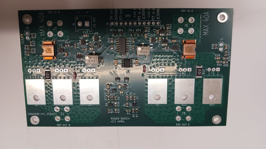
The board is available with SMD components pre-assembled.
Page 1: Current Sensing and Shutdown Logic (Channels A and B)
This page contains the heart of the protection mechanism. The board is split into two identical channels (A and B), allowing independent protection for two separate LDMOS transistors or circuits:
- Current Sensing: Current flows in through the IN_+50VDC connector and passes through a high-precision shunt resistor (WSL4026, 1 mΩ). An INA169 or ZXCT1084, at case of over 50 V use INA293A1 (A=20), IC measures the voltage drop across the resistor and converts it into a current-proportional voltage.
- Resistors R9 and R17 set INA169 the maximum amplication, 24k9 set A=25.
- The calculation example on the schematic shows: 25 A of current corresponds to 3.12 V, and 40 A corresponds to 5.00 V on the A_CURRENT and B_CURRENT lines.
- Comparator and Latch (Trip Logic): The voltage is fed to a TL331 comparator and a 74HC74 D-flip-flop. If the current exceeds the set threshold, the flip-flop latches into a fault state and cuts off the drive lightning-fast.
- Power Switches (Power MOSFETs): Heavy-duty, parallel-connected P-channel Power MOSFETs (IXTP120P065T or SUP60061EL-GE3) act as the actual switch and electronic fuse. They cut off the 50 V supply to the OUT_+50VDC connectors. Use at over 50 V Vds SUP60061EL-GE3.
Page 2: Connectors and Voltage Regulation
This page details how the board physically connects to the rest of the system:
- Main Power Connectors (J1, J2, J3, J4): Heavy-duty 74651173R screw terminals designed for high currents on the 50 VDC inputs and outputs.
- Internal Operating Voltage (U6): An L78L05 linear regulator drops the +12V supply down to +5V for the board's onboard logic. If you have a 3V3 processor (like newer Arduinos), change the regulator to a 3V3 model.
- Control Connector J6 (11-pin male header): The bus through which the board communicates directly with the main motherboard (Control Board). The signals are:
- EN-50V (Enable 50V board)
- SHUTDWN (Open collector type emergency shutdown output)
- FAULT_RST (Logic level pull-up type input to reset the protection)
- GND
- A_CURRENT (Analog voltage signal for Channel A current)
- FAULT_ID_A (CMOS logic level indicator for a Channel A fault)
- A_SHTD and B_SHTD (Connected together so both A and B shutdown at the same time)
- B_CURRENT (Analog voltage signal for Channel B current)
- FAULT_ID_B (CMOS logic level indicator for a Channel B fault)
- Details
- Written by: Jari Ojala
- Category: Uncategorised
- Hits: 531
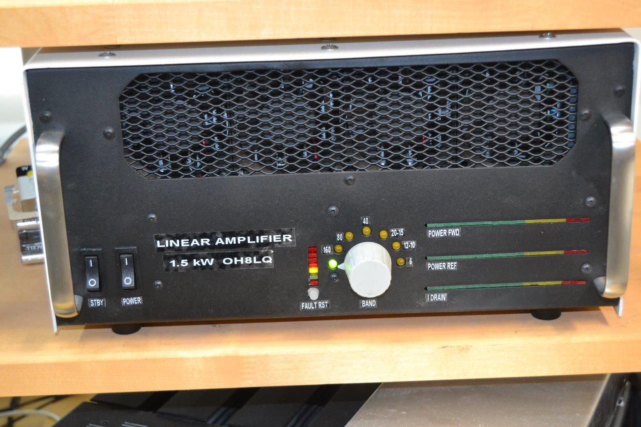
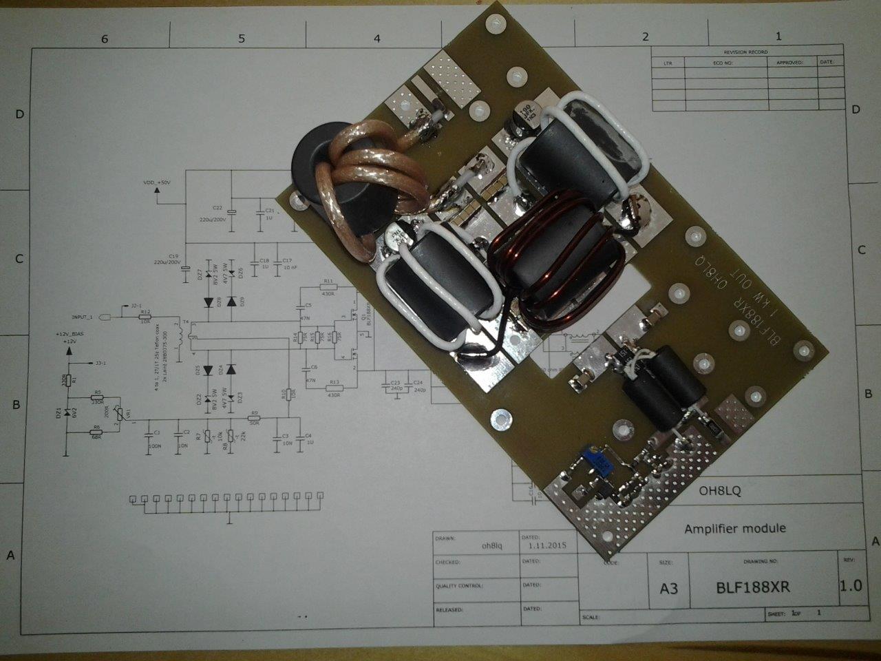
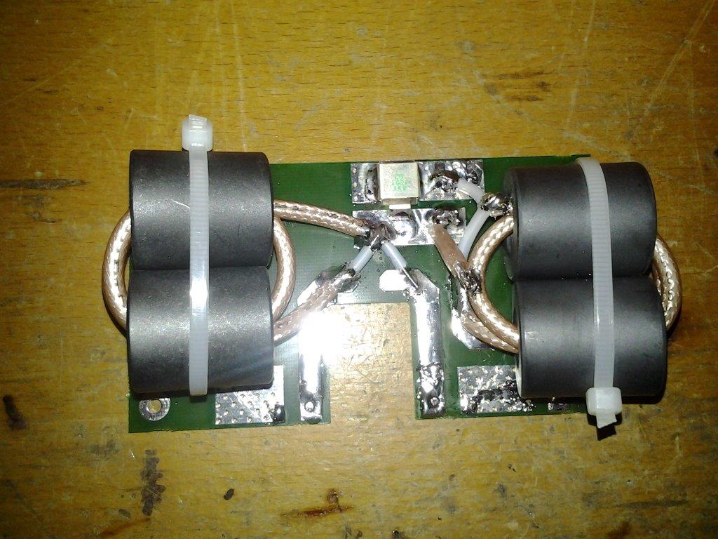
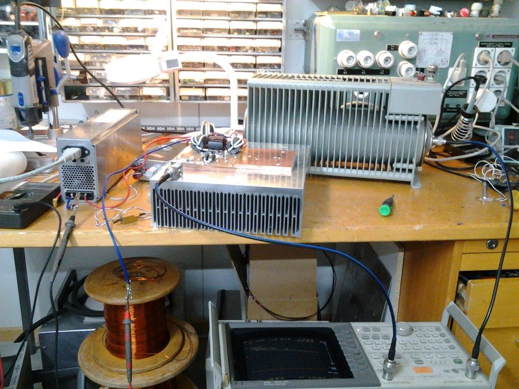
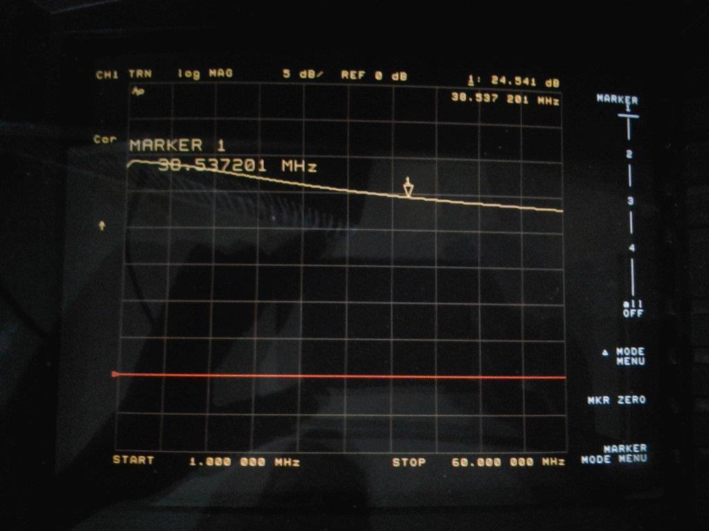
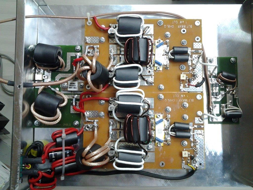
2xBLF188XR LDMOS HF-linear amplifier
- Details
- Written by: Jari Ojala
- Category: Uncategorised
- Hits: 4468
LDMOS Linear amplifier control system.
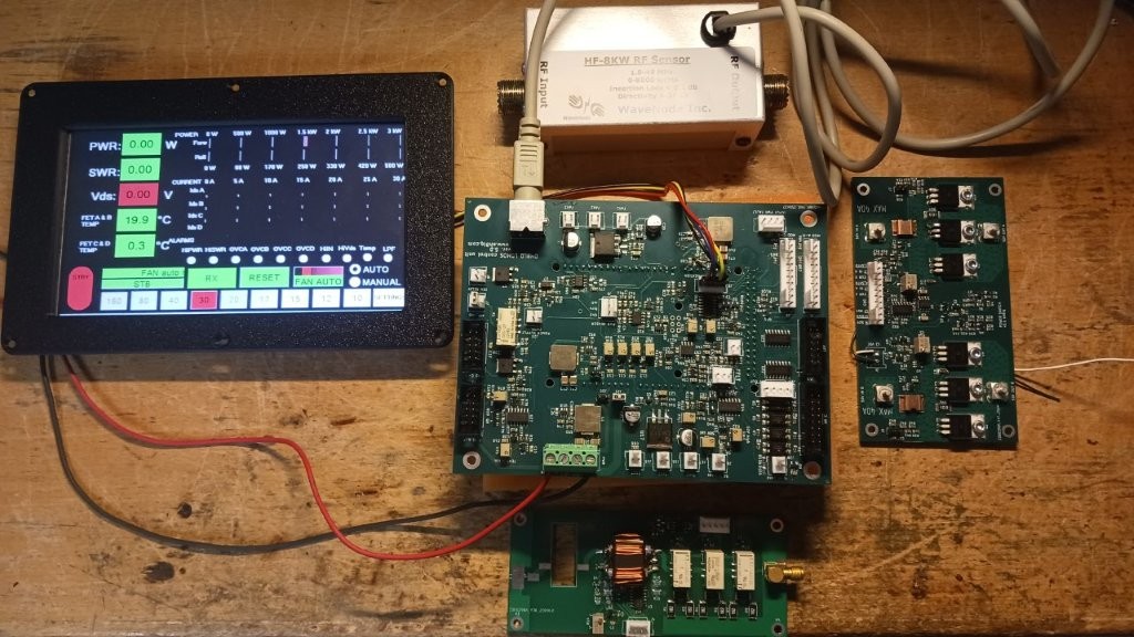
Nextion display, control board, input attenuator and high input power detector, wavenode sensor and DC switch.
Core Features of the Control Board
- Hardware-Level Protection: All critical, high-speed safety trips are built directly into the electronic circuitry (hardware implementation). The software only handles alarm reporting, ensuring lightning-fast protection that remains fully operational regardless of firmware updates or software hangs.
- Dual Arduino Compatibility: The printed circuit board is designed to host either the Arduino DUE or the Arduino Giga WiFi R1 development platform.
- Network Connectivity & Remote Control: When paired with the Arduino Giga, the amplifier gains WiFi connectivity. This enables full remote control and real-time monitoring via a Java-based web interface accessible on any browser.
- Touchscreen Interface: Local operation is handled through a clear, visual Nextion 5" or 7" touchscreen display.
- Over-The-Air (OTA) Updates: Both the Arduino firmware and the Nextion graphical interface files (.tft) can be updated wirelessly over the network, removing the need for physical programming cables. The device can check for the latest versions directly from its own menu.
- Flexible Module Support: The control board scales seamlessly to support amplifiers utilizing 1, 2, or 4 LDMOS modules. The drain current of each module is measured independently, and the main display meter scales are fully adjustable.
- Smart Input Attenuation: A programmable 0–3 dB attenuator can be integrated into the RF input path to balance transceiver drive power on a per-band basis, keeping the sensitive LDMOS gates safe.
- Automatic Band Tracking: Supports automatic frequency and band switching protocols for the most popular transceiver brands, including Yaesu band data, Icom CI-V, and Kenwood CAT.
- Operational Logs & Statistics: The board stores vital usage statistics in memory, tracking the total cumulative power-on time, active transmit runtime, and a dedicated TRX relay cycle counter to monitor component wear.
Hardware
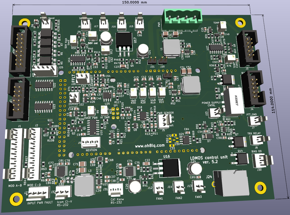
Four layer PWB (Kicad 3D)
Latest version v 5.2 PWB
Version 5.2 control board CAT added for Kenwood and Icom
BOM HTML

If enough people are interested in the circuit board, the board can be ordered in batches, either with or without SMDs installed. The required Arduino can be programmed upon agreement.

PWB and Arduino board (DUE or GIGA uses WiFi and remote possibilties)
Graphic user interface


Four module view

Two module view

One module view
The image displays the Main User Interface (UI) Screen designed for the physical Nextion touch display mounted on the front panel of the amplifier. It contains the exact same control loops and metrics as the web-based remote panel, but formatted specifically for local hardware operation.
The functions and interface elements are arranged as follows:
1. Digital and Analog Meters (Left Side and Top)
- PWR: Live output power readout shown digitally and on a real-time bar graph (0 to 3 kW scale).
- SWR: Antenna line Standing Wave Ratio shown digitally and via a color-coded bar graph (1.0 to 5.0 scale).
- Vds: Direct drain voltage fed to the LDMOS transistors.
- FET A & B TEMP / FET C & D TEMP: Separate real-time temperature telemetry for the two main transistor pairs.
- Ids A, Ids B, Ids C, Ids D: Dedicated horizontal current draw graphs tracking each of the four LDMOS modules individually (0 to 30 A scale).
2. Alarm Status Cluster (Center - ALARMS)
- A dedicated horizontal matrix of status circles that illuminate during hardware faults: HiPWR (over-power), HiSWR (antenna mismatch), OVCA...OVCD (per-module over-current), HiIN (over-drive from transceiver), HiVds (voltage spike), Temp (thermal ceiling tripped), and LPF (improper low-pass filter selection).
3. State Controls and Navigation (Bottom Layout)
- STBY (Red vertical button): Key interlock to alternate the system state between Standby and active Operate mode.
- ERROR Field: A wide text banner that prints clear diagnostic descriptions when safety trips deploy.
- RX: Status block that stays green during reception and turns red to denote active transmission (TX).
- RESET: A clear-fault command to manually override and reset active hardware protection trips after resolving an issue.
- FAN: Speed indicator showing the duty cycle of the active cooling fan network.
- AUTO / MANUAL: Radio toggles to switch between automatic transceiver frequency tracking (via CAT/CI-V bus) and direct manual selection.
- Band Buttons (160 to 10): Direct quick-press keys to manually step through the low-pass filter configurations.
- SETTINGS: Direct page navigation link leading to the main global setup menu analyzed previously.

The image displays the Main Settings Menu for the amplifier controller. This page manages operational parameters, tracks usage statistics, and provides navigation to other submenus.
The functions are divided into three main columns and a bottom row:
1. STATISTICS
- TRX RELAY COUNT: Monitors how many times the transmit/receive (PTT) relays have cycled. This helps track relay wear and tear.
- ON TIME / RUN TIME: Tracks the total cumulative power-on time and active transmit time.
- Yellow reset buttons: Resets the temporary trip meters (RUN TIME TRIP / ON TIME TRIP).
- BAND DATA (YAESU): Selects the transceiver interface protocol. Here, Yaesu is selected (can be toggled to other brands like Icom or Kenwood).
- CURRENT BARS: Configures how many individual transistor current bars are displayed on the main screen.
- POWER SCALE / CURRENT SCALE: Adjusts the maximum scale limits for the analog meters on the main screen.
- Version numbers: Displays current Nextion screen, firmware, and hardware version revisions.
- DIMMER / VOLUME: Sliders to adjust the screen backlight brightness and buzzer sound volume.
2. ATTENUATOR SELECTOR
- INPUT ATTENUATOR: Allows setting a specific attenuation value (in dB) individually for each amateur band (160m to 10m). Since LDMOS gates are highly sensitive, if a transceiver over-drives a specific band, relay-switched physical attenuators can be automatically engaged here (e.g., 1 dB on 80m and 3 dB on 17m in the image).
- Radio buttons at the bottom: Toggles for UTC TIME synchronization, WiFi on/off (disabling the wireless radio), and Remote on/off (enabling network control permissions).
3. ALLOWED BANDS & TIME
- SELECT BANDS: Checkboxes (white circles) for each band. Unchecking a band prevents the amplifier from entering transmit mode on that frequency, serving as a safety interlock.
- DATE / CLOCK: Displays the Real-Time Clock (RTC) status. The image shows the date 13/05/2026 and the active clock time.
4. Bottom Action Buttons
- RESET COUNTERS: Clears the operational statistics.
- SET RTC: Opens the date and time configuration screen.
- LOAD SETTINGS / SAVE OK: Recalls saved configurations from memory or commits new changes permanently to EEPROM.
- Yellow navigation buttons: Direct shortcuts to the submenus previously discussed: CAT Settings (transceiver control), SW update (OTA firmware update), and WiFi Settings.
- EXIT: Closes the settings window and returns to the main operational interface.

The image displays the WiFi Setup configuration menu for the amplifier controller. This interface connects the control board to a local wireless network, enabling remote web browser control and over-the-air updates.
The functions are divided into the following sections:
1. Network Discovery and Connection (WiFi Setup & Search)
- Wifi Networks: A drop-down menu used to scan and select available local wireless networks.
- SSID: The name of the selected wireless network, or a field to manually enter a hidden network name.
- Password: The network security key (hidden behind masked characters ********).
- CONNECT (Green): A button that executes the network login sequence using the entered credentials.
2. Device Identity and Current Connection Status
- Hostname & SAVE: A text input to assign a custom network name to the device (e.g., powerqube). The adjacent SAVE button writes this name to memory.
- Connected WiFi network / Current SSID: Displays the name of the network the controller is currently linked to.
- Current IP: Displays the active network IP address currently assigned to the device (XXX.XXX.XXX.XXX).
3. Static IP Configuration
- Static IP: Toggles between a static IP assignment and automatic network addressing (DHCP).
- Network Fields: Input areas to manually configure the dedicated network settings: Static IP, Netmask, and Gateway.
- SAVE: Commits the manually entered IP, netmask, and gateway values to the hardware.
4. Navigation
- EXIT: Closes the WiFi setup menu and navigates back to the prior interface.
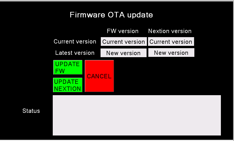
This view displays the Firmware OTA update (Over-The-Air) menu for the amplifier controller. It allows the device firmware and touch screen interface files to be updated wirelessly over the network, eliminating the need to physically connect the control board to a computer with a cable.
The image features the following functions and details:
1. Software Version Tracking (Version Info)
The interface compares the software currently running on the device against the latest available version found on the server for two distinct components:
- FW version: The current version (Current version) and the latest available version (New version) of the main Arduino firmware.
- Nextion version: The current version and the latest available version of the graphical user interface files for the Nextion touch display.
2. Action Buttons
- UPDATE FW: Initiates the wireless firmware update process for the Arduino controller.
- UPDATE NEXTION: Starts downloading and flashing the touch screen interface files (.tft) over the network.
- CANCEL: Aborts the update procedure and exits the menu without applying any changes.
3. Status Tracking
- Status: The large white field at the bottom provides real-time log outputs regarding the update progress (such as connection status, download percentage, and installation phase).
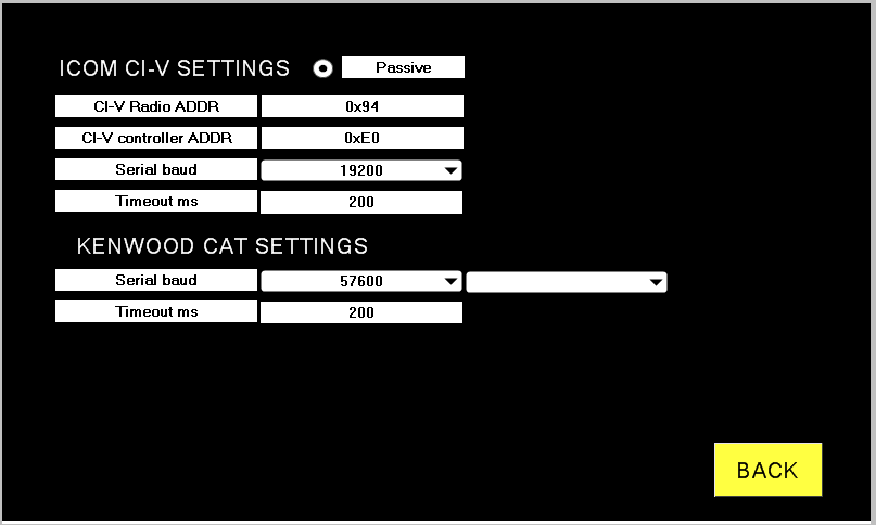
The image displays the radio remote control and communication settings (CAT / CI-V) configuration view for the same OH8LQ controller. This menu configures the amplifier to communicate directly with a connected Icom or Kenwood transceiver for automatic frequency tracking (band switching).
The options are split into two main sections:
1. ICOM CI-V SETTINGS
- Passive/Active selector: Select listener mode or polling mode.
- CI-V Radio ADDR (0x94): The hexadecimal address of the transceiver. The value 0x94 typically corresponds to models like the Icom IC-7300.
- CI-V controller ADDR (0xE0): The unique address of the amplifier's control board (Master) on the bus. The default controller address is set to 0xE0.
- Serial baud (38400): The serial communication speed. It is configured to 38,400 bps. The transceiver's internal settings must match this exact value.
- Timeout ms (200): The connection timeout threshold in milliseconds. If the radio fails to respond within 200 ms, the controller flags a communication error.
2. KENWOOD CAT SETTINGS
- Serial baud (19200): The serial communication speed for a Kenwood transceiver, configured here to 19,200 bps.
- Data bits, Parity, and Stop bits (8N1): The framing configuration for the serial protocol. 8N1 denotes 8 data bits, no parity, and 1 stop bit, which is the standard format for Kenwood.
- Timeout ms (200): The timeout threshold (200 ms) for the Kenwood interface before an error is generated.
The yellow BACK button in the bottom right corner returns the user to the previous menu or main status screen.

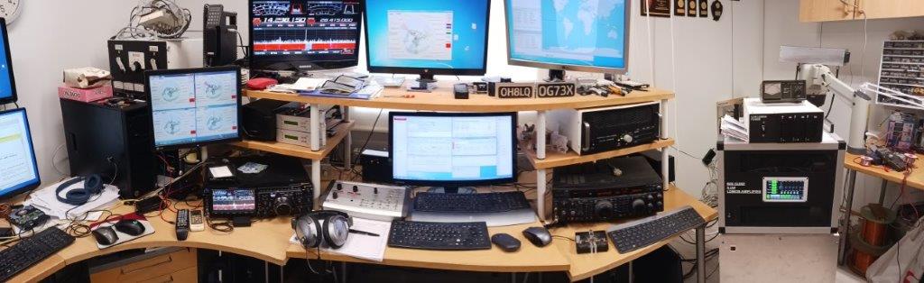
Two amps on display
The scales of the WEB remote panel bars are scaled to the same maximum
value as those of the Nextion display.

The control system runs on an Arduino Giga WiFi R1 board. This connects the amplifier to a local network and lets you monitor its status directly via a web browser.
The functions and user interface elements are divided as follows:
1. Real-Time Meters (Monitoring)
- POWER & SWR: Displays the amplifier output power (W) and the Standing Wave Ratio (SWR) of the antenna line.
- IdsA, IdsB, IdsC, IdsD: Measures the drain current (A) for each of the four LDMOS transistor modules separately. This quickly reveals if a module is unevenly loaded or failing.
- Vds: The supply voltage fed to the transistors (typically around 50 V).
- FET A+B / C+D (°C): Temperature readings for two different pairs of transistor pallets.
- FAN speed: Shows the current speed of the cooling fans, which scales based on power and heat levels.
2. Controls and State Selection
- Band Selection (Band): Buttons for amateur bands from 160m to 10m to switch the low-pass filters (LPF).
- AUTO / MANUAL: Automatic band tracking from the radio (via CAT cable or RF counter) or manual band switching.
- READY STB / OPERATE STATE: Toggle switch to set the amplifier to Standby (STB) or transmission mode (Operate).
- RX/TX: Status indicator light showing when the device is in receive mode.
3. Alarm Indicators
The panel features a comprehensive array of warning lights. While these warnings display on the software interface, the critical safety trips (like high SWR or overcurrent) trigger instantly at the hardware level to protect the expensive LDMOS FETs:
- HiPWR: Excessive output power.
- HiSWR: High reflected power from the antenna.
- OVCA, OVCB, OVCC, OVCD: Over-current (OVC) for each of the four individual modules.
- Hiin: Excessive input drive power from the radio.
- HiVDS: Supply voltage is too high.
- Temp: Overheating condition.
- LPF: Filter error (e.g., incorrect filter selected for the radio's operating frequency).
- RESET FAULT: Button to clear the triggered protection circuits and reset the fault status after troubleshooting.
The bottom of the interface also includes a Theme switcher (Light / Dark) and a Connected indicator, which confirms whether the browser session is actively communicating with the physical amplifier.
Latest remote panel (click link)
Downloadable material
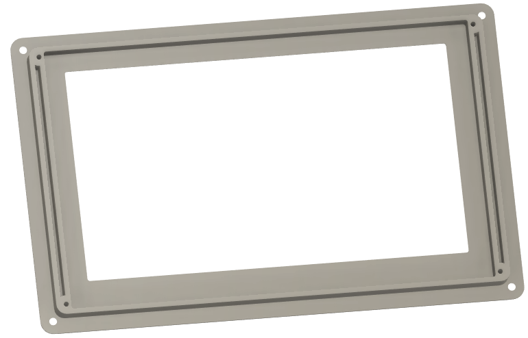
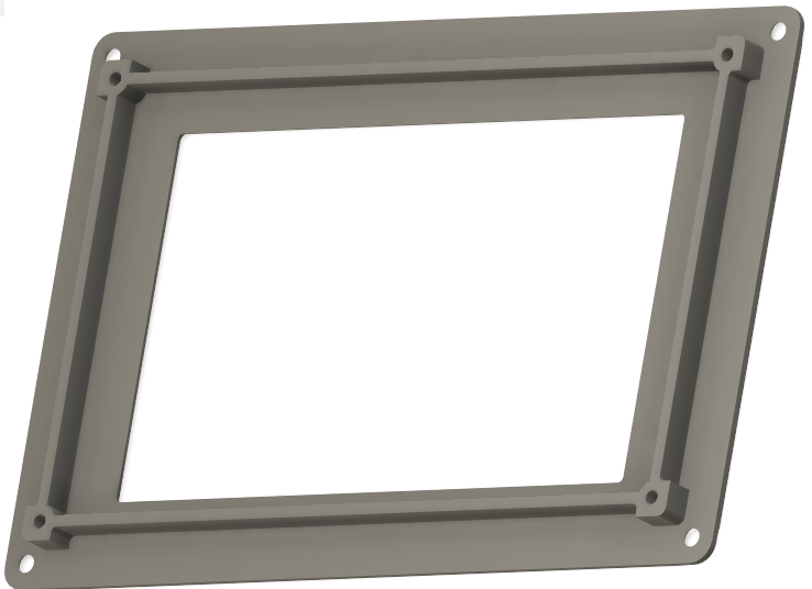
Installation frame 3D-models for Nextion 5" and 7" display
Download 5" TFT OR 7" TFT files


- Details
- Written by: Jari Ojala
- Category: Uncategorised
- Hits: 8968
|
Pin |
Description |
Remarks |
|
1 |
50 V on active LOW |
Output open collector |
|
2 |
Shutdown active LOW |
Output open collector |
|
3 |
Fault reset active LOW |
Output max. 3.3 V |
|
4 |
GND |
|
|
5 |
GND |
|
|
6 |
Current meas module A 0-10 V |
Output analog |
|
7 |
Over current module A active LOW |
input max. 3.3 V |
|
8 |
Shutdown active LOW |
Output open collector |
|
9 |
Current meas module B 0-10 V |
Output analog |
|
10 |
Over current module B active LOW |
input max. 3.3 V |
|
11 |
Shutdown active LOW |
Output open collector |
J1 Connector Vds control module A-B
|
Pin |
Description |
|
|
1 |
50 V on active LOW |
Output open collector |
|
2 |
Shutdown active LOW |
Output open collector |
|
3 |
Fault reset active LOW |
Output max. 3.3 V |
|
4 |
GND |
|
|
5 |
GND |
|
|
6 |
Current meas module C 0-10 V |
Output analog |
|
7 |
Over current module C active LOW |
input max. 3.3 V |
|
8 |
Shutdown active LOW |
Output open collector |
|
9 |
Current meas module D 0-10 V |
Output analog |
|
10 |
Over current module D active LOW |
input max. 3.3 V |
|
11 |
Shutdown active LOW |
Output open collector |
J2 Connector Vds control module C-D
|
1 |
GND |
|
|
2 |
BIAS ON module A Switch bias voltage on. PTT delay 20 ms |
Output Active LOW |
|
3 |
+12 V |
Output |
|
4 |
LM35_A analog in |
Input |
|
5 |
+5 V LM35 Vcc |
Output |
|
6 |
GND |
|
|
7 |
+12 V |
Output |
|
8 |
BIAS ON module B. Switch bias voltage on. PTT delay 20 ms |
Output |
|
9 |
GND |
|
|
10 |
NC |
J3 Connector bias module A
|
1 |
GND |
|
|
2 |
BIAS ON module C. Switch bias voltage on. PTT delay 20 ms |
Output Active LOW |
|
3 |
+12 V |
Output |
|
4 |
LM35_B analog in |
Analog Input |
|
5 |
+5 V LM35 Vcc |
Output |
|
6 |
GND |
|
|
7 |
+12 V |
Output |
|
8 |
BIAS ON module D. Switch bias voltage on. PTT delay 20 ms |
Output |
|
9 |
GND |
|
|
10 |
NC |
J4 Connector bias module B
|
1 |
Reflected 0-13 V (400 W à2,826) |
Input |
|
2 |
Forward 0-13 V (3200 W à7,994V) |
Input |
|
3 |
GND |
J5 Connector Power sensor
|
1 |
Vds scaled |
Input |
|
2 |
GND |
J6 Vds scaled 0-3.3 V
|
1 |
+12 V |
|
|
2 |
Relay (open collector) |
Output |
J8 Connector J8 RTX-relay control
|
1 |
PTT active LOW |
Input |
|
2 |
GND |
J7 Connector PTT
|
1 |
GND |
|
|
2 |
Serial RX TTL 5V |
Input |
|
3 |
Serial TX TTL 5V |
Output |
|
4 |
+5 V 1.5 A |
J9 Connector Nextion display
|
1 |
NC |
|
|
2 |
GND |
|
|
3 |
PTT |
Input |
|
4 |
TX INH |
Input |
|
5 |
GND |
|
|
6 |
NC |
|
|
7 |
BAND A |
Input |
|
8 |
NC |
|
|
9 |
BAND B |
Input |
|
10 |
NC |
|
|
11 |
BAND C |
Input |
|
12 |
NC |
|
|
13 |
BAND D |
Input |
|
14 |
GND 1 |
|
|
15 |
TX INH |
Input |
|
16 |
NC |
J10 Yaesu Linear port
|
1 |
+12 V |
|
|
2 |
160 m (open collector) |
Output |
|
3 |
80 m (open collector) |
Output |
|
4 |
60 m (open collector) |
Output |
|
5 |
40 m (open collector) |
Output |
|
6 |
30 m (open collector) |
Output |
|
7 |
20 m (open collector) |
Output |
|
8 |
17 m (open collector) |
Output |
|
9 |
15 m (open collector) |
Output |
|
10 |
12 m (open collector) |
Output |
|
11 |
10 m (open collector) |
Output |
|
12 |
NC |
J11 LPF control
|
1 |
FAN+ 5-12 V temperature controlled A |
Output |
|
2 |
GND |
J12 FAN power
|
1 |
FAN+ 5-12 V temperature controlled A |
Output |
|
2 |
GND |
J13 FAN power
|
1 |
FAN+ 5-12 V temperature controlled A |
Output |
|
2 |
GND |
J14 FAN power
|
1 |
FAN+ 5-12 V temperature controlled B |
Output |
|
2 |
GND |
J15 FAN power
|
1 |
FAN+ 5-12 V temperature controlled B |
Output |
|
2 |
GND |
J16 FAN power
|
1 |
FAN+ 5-12 V temperature controlled B |
Output |
|
2 |
GND |
J17 FAN power
|
1 |
+12 V 2 A |
Input |
|
2 |
+5 V 500 mA |
Output |
|
3 |
+3.3 V 500 mA |
Output |
|
4 |
GND |
J18 Power connector
|
1 |
Power signal 0-3.3 V |
Input |
|
2 |
GND |
J22 Harmonic load power sensor
|
1 |
Closing relay max 1 A |
Output |
|
2 |
COM |
Output |
J23 Vds Power supply control
|
1 |
REFL |
Input |
|
2 |
REFL |
Input |
|
3 |
FORW |
Input |
|
4 |
FORW |
Input |
|
5 |
GND |
|
|
6 |
GND |
J24 WaveNode sensor MiniDIN
|
1 |
+12 V |
|
|
2 |
Input ATT control 1 (open collector) |
Output |
|
3 |
Input ATT control 2 (open collector) |
Output |
|
4 |
Input ATT control 3 (open collector) |
Output |
|
5 |
GND |
J25 Input attenuator control
|
1 |
Forwarding power 0-10 V |
Input |
|
2 |
Reflected power 0-10 V |
Input |
|
3 |
GND |
J26 LPF-fault sensor
|
1 |
Shutdown active LOW |
input |
|
2 |
Input over power detected active LOW |
input |
|
3 |
Fault reset active LOW |
output |
|
4 |
GND |
J27 Input over power protection
|
1 |
BAND signal 0-10 V |
Input (ICOM band voltages) |
|
2 |
GND |
J28 ICOM band selector
|
1 |
RXD |
Input |
|
2 |
GND |
|
|
3 |
ESP_PD (power down) |
Output |
|
4 |
NC |
|
|
5 |
NC |
|
|
6 |
NC |
|
|
7 |
+3V3 |
Output |
|
8 |
TXD |
Output |
J29 ESP32 Wifi module
|
J19 |
+3V3 to Arduino |
No Connect |
|
J20 |
+5 V to arduino |
No connect |
|
J21 |
+ 12 V Vcc to Arduino |
Closed (feed 12 V to Arduino) |
Jumpers (set arduino voltages)
Calibration
|
Trimmer |
Adjustment |
Cause |
|
R9 |
Over Power |
Set point to shutdown amplifier |
|
R10 |
Ids A Calibration |
Display bar level setting |
|
R19 |
Ids B Calibration |
Display bar level setting |
|
R23 |
Hi SWR Calibration |
Set point to shutdown amplifier |
|
R29 |
Ids C Calibration |
Display bar level setting |
|
R30 |
Ids D Calibration |
Display bar level setting |
|
R31 |
Vds measurement calibration |
Display bar level setting |
|
R32 |
Vds Upper limit calibration |
Set point to shutdown amplifier |
|
R75 |
Max temperature A-sensor |
Set point to shutdown amplifier |
|
R76 |
Max temperature B-sensor |
Set point to shutdown amplifier |
|
R113 |
LPF Fault SWR detection |
Set point to shutdown amplifier |
Trimmers