Uncategorised
- Details
- Written by: Jari Ojala
- Category: Uncategorised
- Hits: 7002
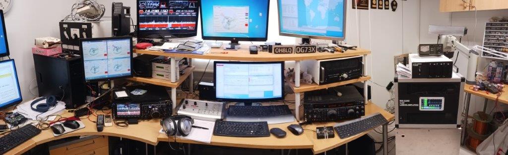
QSL info
OH8L LoTW and direct (SASE)
OH8LQ Lotw and direct (SASE)
OG73X LoTW and direct (SASE)
- Details
- Written by: Jari Ojala
- Category: Uncategorised
- Hits: 1149
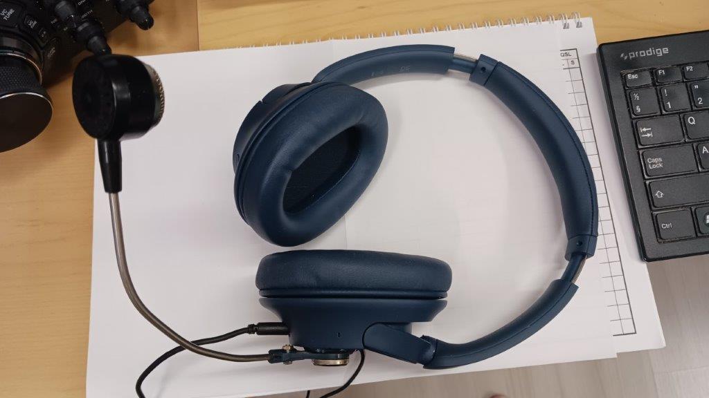
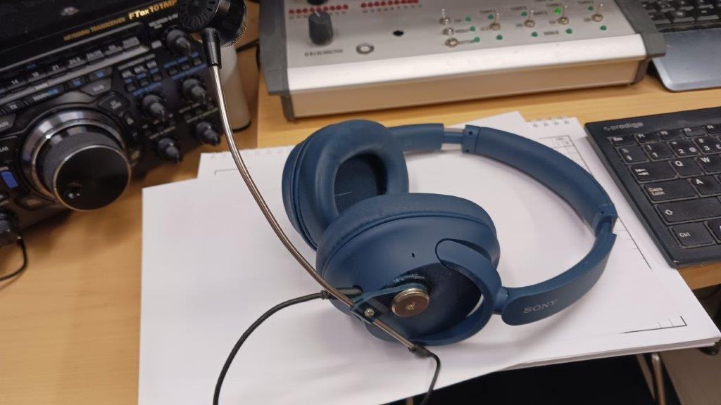
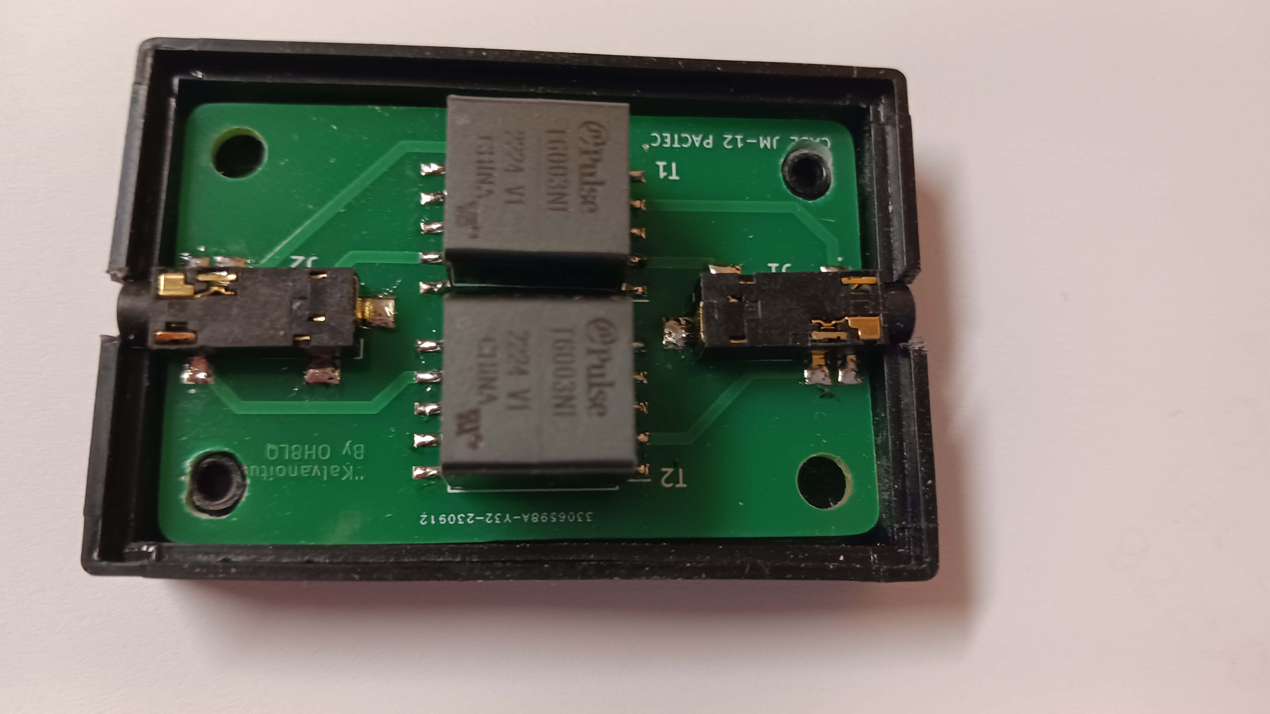
Galvanic stereo Isolator/
"galvanoitu erotin"
- Details
- Written by: Jari Ojala
- Category: Uncategorised
- Hits: 4649
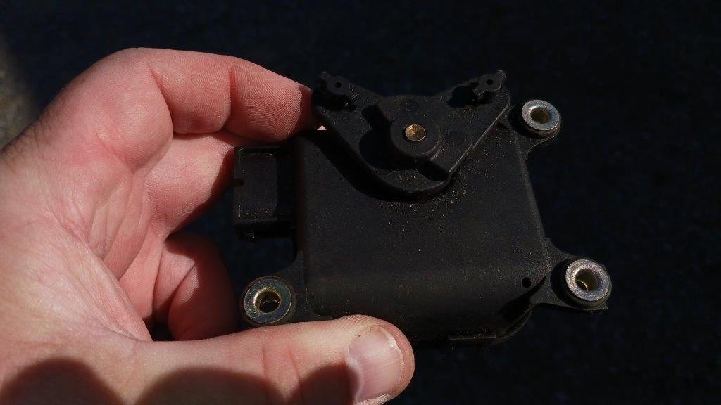
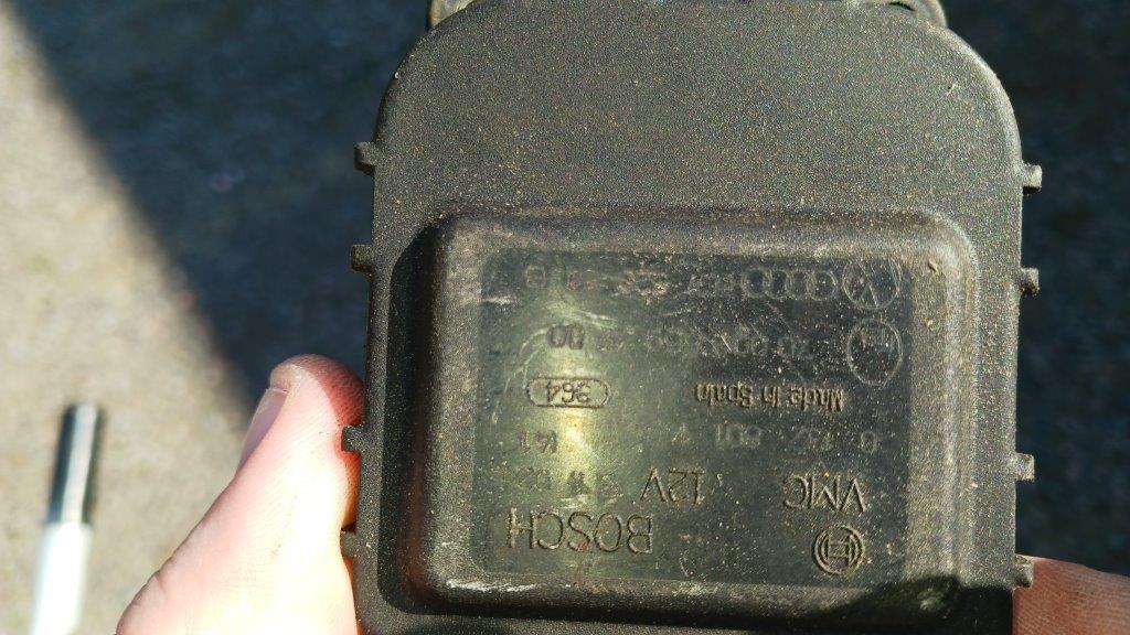
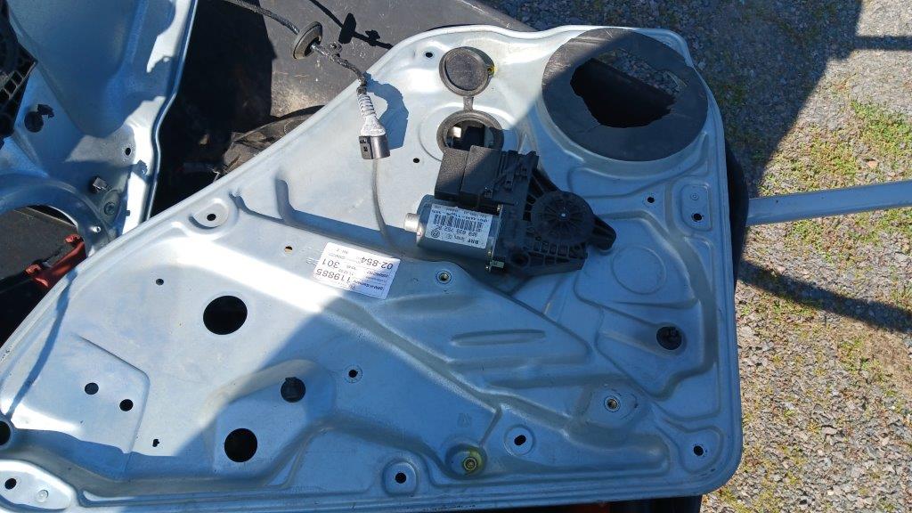
Kuvissa näkyviä osia puretusta Passatti farkusta.
Kysy 0400 815634 tai jari.ojala (at) oh8lq.com
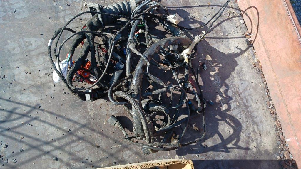
AVF koneen johtosarja täydellinen!
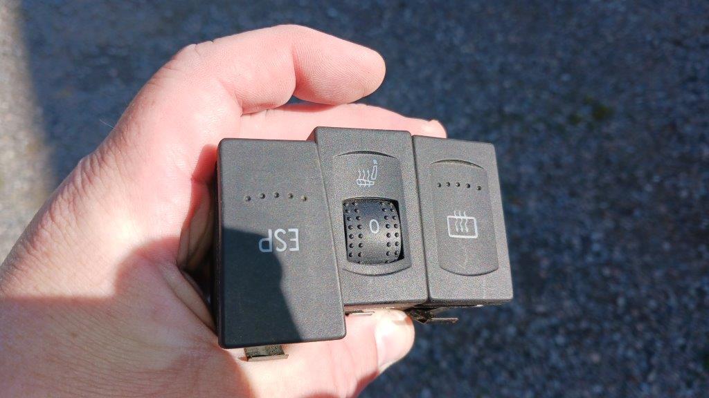
Kytkimiä
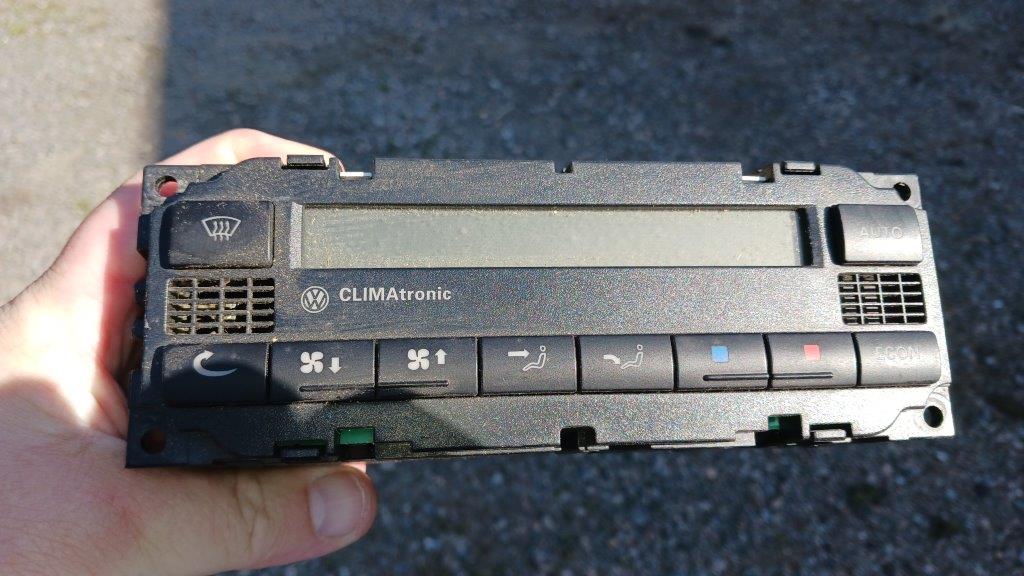
Climatronic paneeli
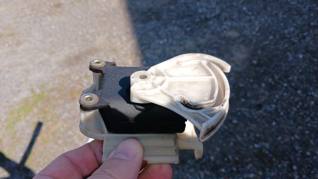
Lämppärin servoja
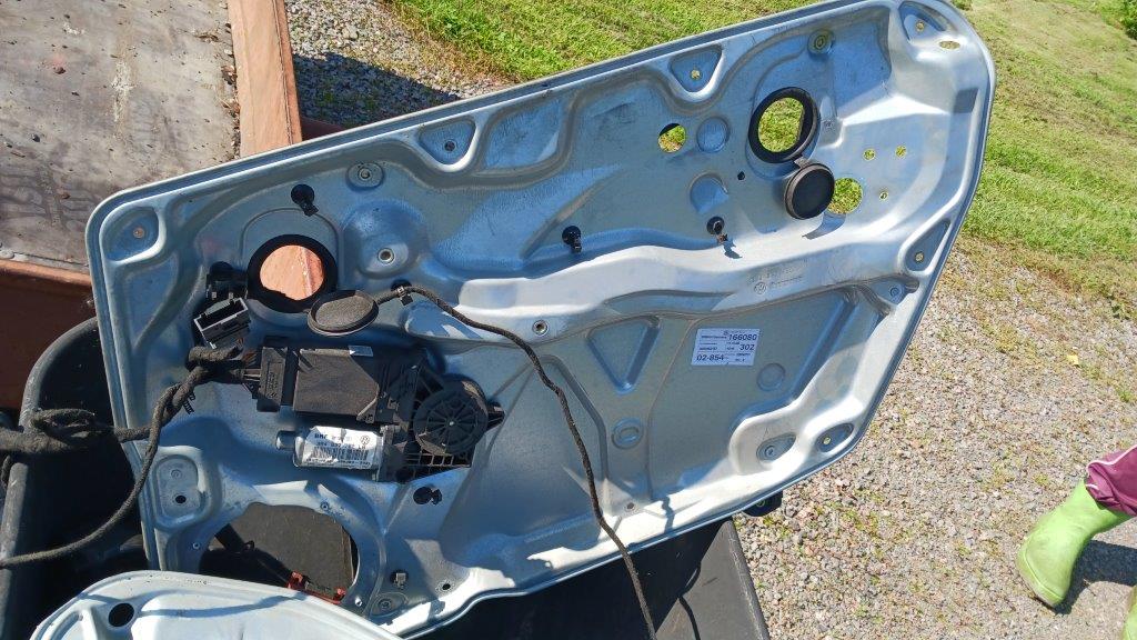
Kuskin oven lasinnostin moottori/pelti
Takaoven lasinnostin +pelti
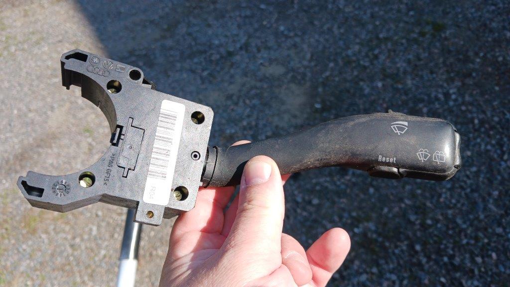
Lasinpyyhkijän vipu
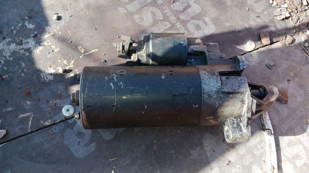
Starttimoottori
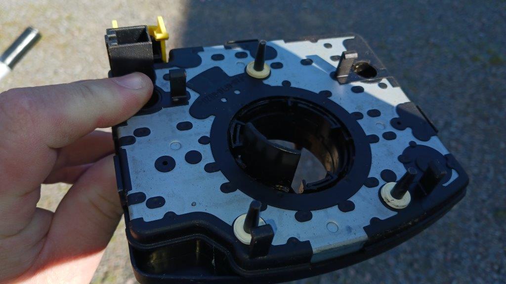
Ratin turvatyynyn kierre johto?!
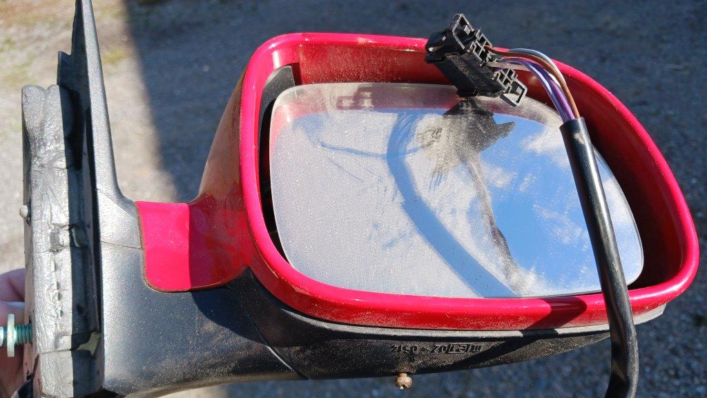
Sivupeili
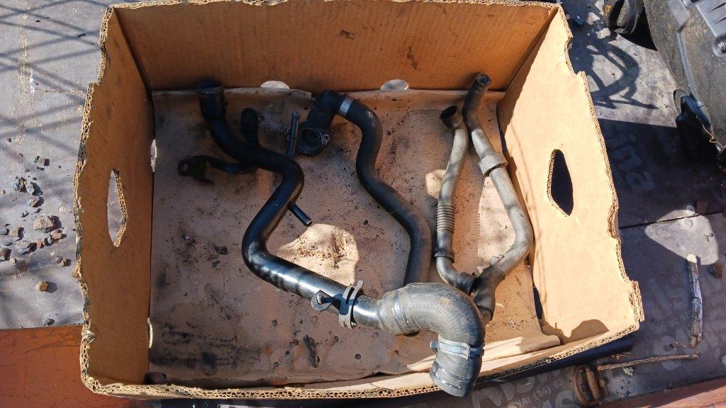
Sekalaisia putkia, kuvassa ei ole EGR:n lauhdutin ja putket, löytyvät myös...
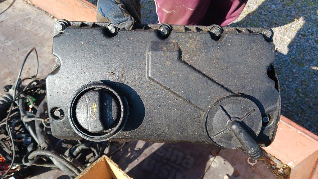
Venttiilikopankansi
Lisäksi löytyy yksi 100tkm ajettu pumppusuutin ja ABS-pumppuyksikkö!!